Difference between revisions of "Aufgaben:Exercise 1.6: Cyclic Redundancy Check"
| (25 intermediate revisions by 4 users not shown) | |||
| Line 1: | Line 1: | ||
| − | {{quiz-Header|Buchseite= | + | {{quiz-Header|Buchseite=Examples_of_Communication_Systems/ISDN_Primary_Multiplex_Connection |
}} | }} | ||
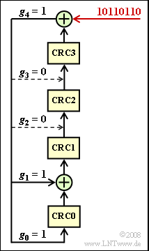
| − | [[File:P_ID1626__Bei_A_1_6.png|right|frame| | + | [[File:P_ID1626__Bei_A_1_6.png|right|frame|CRC4 checksum formation]] |
| − | + | The synchronization happens at the primary multiplex connection in each case in synchronization channel "$0$" of each frame: | |
| + | # For odd time frames (number 1, 3, ... , 15) this transmits the so-called "frame password" with the fixed bit pattern $\rm X001\hspace{0.05cm} 1011$. | ||
| + | # Each even frame (with number 2, 4, ... , 16) on the other hand contains the "message word" $\rm X1DN\hspace{0.05cm}YYYY$. | ||
| + | # Error messages are signaled via the $\rm D$ bit and the $\rm N$ bit. The four $\rm Y$ bits are reserved for service functions. | ||
| − | |||
| − | + | The $\rm X$ bit is obtained in each case by the "CRC4 method", the implementation of which is shown in the diagram: | |
| + | *From eight input bits each - in the entire exercise the bit sequence "$\rm 1011\hspace{0.05cm} 0110$" is assumed for this purpose - the four check bits $\rm CRC3$, ... , $\rm CRC0$ are obtained by modulo-2 additions and shifts, which are added to the input word in this order. | ||
| + | |||
| + | *Before the first bit is shifted into the register, all registers are filled with zeros: | ||
:$${\rm CRC3 = CRC2 =CRC1 =CRC0 = 0}\hspace{0.05cm}.$$ | :$${\rm CRC3 = CRC2 =CRC1 =CRC0 = 0}\hspace{0.05cm}.$$ | ||
| − | + | *After eight shift clocks, the four registers $\rm CRC3$, ... , $\rm CRC0$ contains the CRC4 checksum. | |
| + | |||
| + | |||
| − | + | The taps of the shift register are $g_{0} = 1, \ g_{1} = 1, \ g_{2} = 0, \ g_{3} = 0$ and $g_{4} = 1$. | |
| + | *The corresponding generator polynomial is: | ||
:$$G(D) = D^4 + D +1 \hspace{0.05cm}.$$ | :$$G(D) = D^4 + D +1 \hspace{0.05cm}.$$ | ||
| − | + | *The CRC4 checksum on the transmission side is also obtained as the "'''remainder'''" of the polynomial division | |
:$$(D^{11} +D^{9} +D^{8}+D^{6}+D^{5})/G(D) \hspace{0.05cm}.$$ | :$$(D^{11} +D^{9} +D^{8}+D^{6}+D^{5})/G(D) \hspace{0.05cm}.$$ | ||
| − | + | *The divisor polynomial results from the input sequence and four appended zeros: "$\rm 1011\hspace{0.09cm} 0110\hspace{0.09cm} 0000$". | |
| − | + | ||
| + | |||
| + | The CRC4 check at the receiver according to subtask '''(4)''' can also be represented by a polynomial division. It can be implemented by a shift register structure in a similar way as the CRC4 checksum is obtained at the transmitting end. | ||
| + | |||
| + | |||
| + | |||
| + | |||
| + | |||
| + | Notes: | ||
| + | |||
| + | *The exercise belongs to the chapter [[Examples_of_Communication_Systems/ISDN_Primary_Multiplex_Connection|"ISDN Primary Multiplex Connection"]] . | ||
| + | *To solve the exercise, some basic knowledge of [[Channel_Coding|"Channel Coding"]] is required. | ||
| + | |||
| − | |||
| − | + | ===Questions=== | |
| − | === | ||
<quiz display=simple> | <quiz display=simple> | ||
| − | { | + | {Which result $E(D)$ and which remainder $R(D)$ results from the polynomial division |
| − | $(D^{11} + D^{9} + D^{8} + D^{6} + D^{5}) : (D^{4} + D + 1)? | + | $(D^{11} + D^{9} + D^{8} + D^{6} + D^{5}) : (D^{4} + D + 1)$ ? |
| − | |type=" | + | |type="()"} |
| − | - $E(D) = D^{5} + D^{3} + 1, R(D) = D^{3} + D$, | + | - $E(D) = D^{5} + D^{3} + 1, \hspace{2.13cm}R(D) = D^{3} + D$, |
| − | + $E(D) = D^{7} + D^{5} + D^{3} + 1, R(D) = D^{3} + D + 1$, | + | + $E(D) = D^{7} + D^{5} + D^{3} + 1, \hspace{1cm}R(D) = D^{3} + D + 1$, |
| − | - $E(D) = D^{7} + D^{5} + D^{3} + 1, R(D) = 0$. | + | - $E(D) = D^{7} + D^{5} + D^{3} + 1, \hspace{1cm}R(D) = 0$. |
| − | { | + | {What is the CRC checksum in the present case? |
|type="{}"} | |type="{}"} | ||
| − | $CRC0 \ = \ $ { 1 3% } | + | $\rm CRC0 \ = \ $ { 1 3% } |
| − | $CRC1 \ = \ $ { 1 3% } | + | $\rm CRC1 \ = \ $ { 1 3% } |
| − | $CRC2 \ = \ $ { 0 | + | $\rm CRC2 \ = \ $ { 0. } |
| − | $CRC3 \ = \ $ { 1 3% } | + | $\rm CRC3 \ = \ $ { 1 3% } |
| − | { | + | {The following bit sequences arrive at the receiver, eight information bits each plus $\text{ (CRC3, CRC2, CRC1,CRC0)}$. <br>What bit sequences indicate that there is no bit error? |
|type="[]"} | |type="[]"} | ||
| − | - | + | - $1011 \hspace{0.1cm}0010\hspace{0.08cm} 1011$, |
| − | + | + | + $1011 \hspace{0.1cm}0110 \hspace{0.08cm}1011$, |
| − | - | + | - $1011 \hspace{0.1cm}0110\hspace{0.08cm} 1001$. |
| − | { | + | {Which of the following received bit sequences were falsified during transmission? |
|type="[]"} | |type="[]"} | ||
| − | + | + | + $0000 \hspace{0.1cm}0111 \hspace{0.1cm}0010$, |
| − | - | + | - $0000 \hspace{0.1cm}1111\hspace{0.1cm} 0010$, |
| − | + | + | + $0000\hspace{0.1cm} 1111\hspace{0.1cm} 1010$. |
</quiz> | </quiz> | ||
| − | === | + | ===Solution=== |
{{ML-Kopf}} | {{ML-Kopf}} | ||
| − | '''(1)''' | + | '''(1)''' The <u>Solution 2</u> is correct: |
| − | :$$E(D) \cdot G(D) \ = \ (D^7+ D^5+D^3+1)\cdot (D^4+ D+1) \ = | + | *Due to the largest numerator exponent $(D^{11})$ and the highest denominator exponent $(D^{4})$, the first suggestion $E(D) = D^{5} + D^{3} + 1$ can be excluded as the result ⇒ $E(D) = D^{7} + D^{5} + D^{3} + 1$. |
| − | + | ||
| − | + | *Modulo-2 multiplication of $E(D)$ by the generator polynomial $G(D) = D^{4} + D + 1$ yields: | |
| − | + | :$$E(D) \cdot G(D) \ = \ (D^7+ D^5+D^3+1)\cdot (D^4+ D+1) \ = D^{11}+D^8+D^7+D^9+D^6+D^5+D^7+D^4+D^3+D^4+ D+1 \hspace{0.05cm}.$$ | |
| + | *It must be taken into account here that for modulo-2 calculations $D^{4} + D^{4} = 0$. This results in the following remainder: | ||
:$$R(D) = D^{11}+D^9+D^8+D^6+D^5- E(D) \cdot G(D) = D^3+D+1 \hspace{0.05cm}.$$ | :$$R(D) = D^{11}+D^9+D^8+D^6+D^5- E(D) \cdot G(D) = D^3+D+1 \hspace{0.05cm}.$$ | ||
| − | |||
| − | |||
| − | |||
| − | |||
| − | |||
| − | |||
| − | '''(3)''' | + | [[File:EN_Bei_A_1_6b_ML.png|right|frame|Register assignments for CRC4]] |
| + | '''(2)''' From the result of subtask '''(1)''' follows: | ||
| + | :$${\rm CRC0 = 1},\hspace{0.2cm}{\rm CRC1 = 1},\hspace{0.2cm}{\rm CRC2 = 0},\hspace{0.2cm}{\rm CRC3 = 1}\hspace{0.05cm}.$$ | ||
| + | *The table shows a second way of solution: | ||
| + | |||
| + | *It contains the register assignments of the given circuit at times $0$, ... , $8$. | ||
| + | |||
| + | |||
| + | |||
| + | '''(3)''' Only <u>solution 2</u> is correct: | ||
| + | *The receiver divides the polynomial $P(D)$ of the received sequence by the generator polynomial $G(D)$. | ||
| + | |||
| + | *If this modulo-2 division returns the remainder $R(D) = 0$, then all $12$ bits were transmitted correctly. | ||
| + | |||
| + | *This is true for the second solution, as a comparison with subtasks '''(1)''' and '''(2)''' shows. It is valid without remainder: | ||
:$$(D^{11}+D^9+D^8+D^6+D^5+D^3+D+1) : (D^4+ D+1)= D^7+D^5+D^3+1 \hspace{0.05cm}.$$ | :$$(D^{11}+D^9+D^8+D^6+D^5+D^3+D+1) : (D^4+ D+1)= D^7+D^5+D^3+1 \hspace{0.05cm}.$$ | ||
| − | + | *In solution 1 the 6th information bit was falsified, in solution 3 the CRC1 bit. | |
| + | |||
| + | |||
| + | |||
| + | '''(4)''' <u>Solutions 1 and 3</u> are correct: | ||
| + | [[File:EN_Bei_A_1_6d.png|right|frame|Polynomial division of the three received sequences]] | ||
| + | |||
| + | *The diagram illustrates the modulo-2 divisions for the given received sequences in simplified form (with zeros and ones). | ||
| + | *You can see that only for sequence 2 the division is possible without remainder. | ||
| − | + | *In written form, is possible the polynomial divisions are: | |
| − | + | $$\ (1) \ \hspace{0.2cm}(D^6+D^5+D^4+1) : (D^4+ D+1)$$ | |
| − | + | :$$\hspace{0.3cm}\Rightarrow \hspace{0.3cm}\text{remainder:}\hspace{0.15cm}D^3+ D+1\hspace{0.05cm},$$ | |
| − | + | $$\ (2) \ \hspace{0.2cm}(D^7+D^6+D^5+D^4+1) : (D^4+ D+1)$$ | |
| − | + | :$$\hspace{0.3cm}\Rightarrow \hspace{0.3cm}\text{remainder:}\hspace{0.15cm}0\hspace{0.05cm},$$ | |
| − | + | $$\ (3) \ \hspace{0.2cm}(D^7+D^6+D^5+D^4+D^3+1) : (D^4+ D+1)$$ | |
| + | :$$\hspace{0.3cm}\Rightarrow \hspace{0.3cm}\text{remainder:}\hspace{0.15cm}D^3\hspace{0.05cm}.$$ | ||
{{ML-Fuß}} | {{ML-Fuß}} | ||
| Line 90: | Line 126: | ||
| − | [[Category: | + | [[Category:Examples of Communication Systems: Exercises|^1.3 ISDN Primary Multiplex Line^]] |
| − | ^]] | ||
Latest revision as of 17:31, 23 January 2023
The synchronization happens at the primary multiplex connection in each case in synchronization channel "$0$" of each frame:
- For odd time frames (number 1, 3, ... , 15) this transmits the so-called "frame password" with the fixed bit pattern $\rm X001\hspace{0.05cm} 1011$.
- Each even frame (with number 2, 4, ... , 16) on the other hand contains the "message word" $\rm X1DN\hspace{0.05cm}YYYY$.
- Error messages are signaled via the $\rm D$ bit and the $\rm N$ bit. The four $\rm Y$ bits are reserved for service functions.
The $\rm X$ bit is obtained in each case by the "CRC4 method", the implementation of which is shown in the diagram:
- From eight input bits each - in the entire exercise the bit sequence "$\rm 1011\hspace{0.05cm} 0110$" is assumed for this purpose - the four check bits $\rm CRC3$, ... , $\rm CRC0$ are obtained by modulo-2 additions and shifts, which are added to the input word in this order.
- Before the first bit is shifted into the register, all registers are filled with zeros:
- $${\rm CRC3 = CRC2 =CRC1 =CRC0 = 0}\hspace{0.05cm}.$$
- After eight shift clocks, the four registers $\rm CRC3$, ... , $\rm CRC0$ contains the CRC4 checksum.
The taps of the shift register are $g_{0} = 1, \ g_{1} = 1, \ g_{2} = 0, \ g_{3} = 0$ and $g_{4} = 1$.
- The corresponding generator polynomial is:
- $$G(D) = D^4 + D +1 \hspace{0.05cm}.$$
- The CRC4 checksum on the transmission side is also obtained as the "remainder" of the polynomial division
- $$(D^{11} +D^{9} +D^{8}+D^{6}+D^{5})/G(D) \hspace{0.05cm}.$$
- The divisor polynomial results from the input sequence and four appended zeros: "$\rm 1011\hspace{0.09cm} 0110\hspace{0.09cm} 0000$".
The CRC4 check at the receiver according to subtask (4) can also be represented by a polynomial division. It can be implemented by a shift register structure in a similar way as the CRC4 checksum is obtained at the transmitting end.
Notes:
- The exercise belongs to the chapter "ISDN Primary Multiplex Connection" .
- To solve the exercise, some basic knowledge of "Channel Coding" is required.
Questions
Solution
(1) The Solution 2 is correct:
- Due to the largest numerator exponent $(D^{11})$ and the highest denominator exponent $(D^{4})$, the first suggestion $E(D) = D^{5} + D^{3} + 1$ can be excluded as the result ⇒ $E(D) = D^{7} + D^{5} + D^{3} + 1$.
- Modulo-2 multiplication of $E(D)$ by the generator polynomial $G(D) = D^{4} + D + 1$ yields:
- $$E(D) \cdot G(D) \ = \ (D^7+ D^5+D^3+1)\cdot (D^4+ D+1) \ = D^{11}+D^8+D^7+D^9+D^6+D^5+D^7+D^4+D^3+D^4+ D+1 \hspace{0.05cm}.$$
- It must be taken into account here that for modulo-2 calculations $D^{4} + D^{4} = 0$. This results in the following remainder:
- $$R(D) = D^{11}+D^9+D^8+D^6+D^5- E(D) \cdot G(D) = D^3+D+1 \hspace{0.05cm}.$$
(2) From the result of subtask (1) follows:
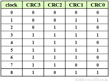
- $${\rm CRC0 = 1},\hspace{0.2cm}{\rm CRC1 = 1},\hspace{0.2cm}{\rm CRC2 = 0},\hspace{0.2cm}{\rm CRC3 = 1}\hspace{0.05cm}.$$
- The table shows a second way of solution:
- It contains the register assignments of the given circuit at times $0$, ... , $8$.
(3) Only solution 2 is correct:
- The receiver divides the polynomial $P(D)$ of the received sequence by the generator polynomial $G(D)$.
- If this modulo-2 division returns the remainder $R(D) = 0$, then all $12$ bits were transmitted correctly.
- This is true for the second solution, as a comparison with subtasks (1) and (2) shows. It is valid without remainder:
- $$(D^{11}+D^9+D^8+D^6+D^5+D^3+D+1) : (D^4+ D+1)= D^7+D^5+D^3+1 \hspace{0.05cm}.$$
- In solution 1 the 6th information bit was falsified, in solution 3 the CRC1 bit.
(4) Solutions 1 and 3 are correct:
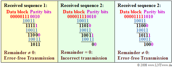
- The diagram illustrates the modulo-2 divisions for the given received sequences in simplified form (with zeros and ones).
- You can see that only for sequence 2 the division is possible without remainder.
- In written form, is possible the polynomial divisions are:
$$\ (1) \ \hspace{0.2cm}(D^6+D^5+D^4+1) : (D^4+ D+1)$$
- $$\hspace{0.3cm}\Rightarrow \hspace{0.3cm}\text{remainder:}\hspace{0.15cm}D^3+ D+1\hspace{0.05cm},$$
$$\ (2) \ \hspace{0.2cm}(D^7+D^6+D^5+D^4+1) : (D^4+ D+1)$$
- $$\hspace{0.3cm}\Rightarrow \hspace{0.3cm}\text{remainder:}\hspace{0.15cm}0\hspace{0.05cm},$$
$$\ (3) \ \hspace{0.2cm}(D^7+D^6+D^5+D^4+D^3+1) : (D^4+ D+1)$$
- $$\hspace{0.3cm}\Rightarrow \hspace{0.3cm}\text{remainder:}\hspace{0.15cm}D^3\hspace{0.05cm}.$$


